Marketing of modern graphics processors involves comparing many low-level performance metrics. For example, our PowerVR GPUs are commonly compared based on GFLOPS (a measure of computing throughput), triangles per second (a measure of geometry throughput), pixels per second and texels per second (measures of fill rate).
In addition to these more traditional metrics, it has become commonplace for companies to describe their architectures in terms of the number of cores they include. Despite being computing terminology with an established history, the meaning of this term has become distorted by GPU marketing. That said, language is malleable and terms get updated over time to reflect their common use. I’ll come back to that common use part.
What is a core?
It depends. Core count traditionally tracks the number of front-ends in a processor. Without complicating it too much, the front-end is responsible for scheduling and dispatch of threads of execution. In almost all modern GPUs, again simplifying things a lot to make the point, there are multiple schedulers and associated dispatch logic, all sitting in front of their own compute resources to schedule work on.
Each scheduler keeps track of a number of threads that need to execute, running a single instruction for a single program in a single cycle. That notion of a single instruction pointer which runs a program on a set of compute resources, regardless of the number of threads or how the compute resources are shared, is the traditional definition of a core.
However, we’ve also used the term to describe whole instances of our Series5 SGX GPUs. In an SGX544MP3 for example, there are 3 complete instances of the SGX544 IP, duplicating all GPU resources, and we call that MP3 configuration a 3 core GPU.
Creative accounting
So, with the rapid increase in the number of CPU cores in modern mobile designs, GPU vendors want to put out that message that a GPU is a multi-core design too, and many of our competitors take an extra advantage by counting individual ALU pipelines as cores. Those pipelines can’t be scheduled completely independently of each other, and so they run the same instruction per cycle as their peers in SIMD fashion. No separate front-end or individual instruction pointer as we’ve outlined, but nonetheless marketed as a core.
Let’s describe PowerVR Rogue in the same way, from the basic building block of the Unified Shading Cluster down to its individual pipelines, and see what number of cores comes out.
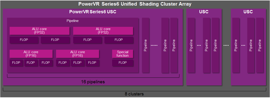
PowerVR Rogue USC
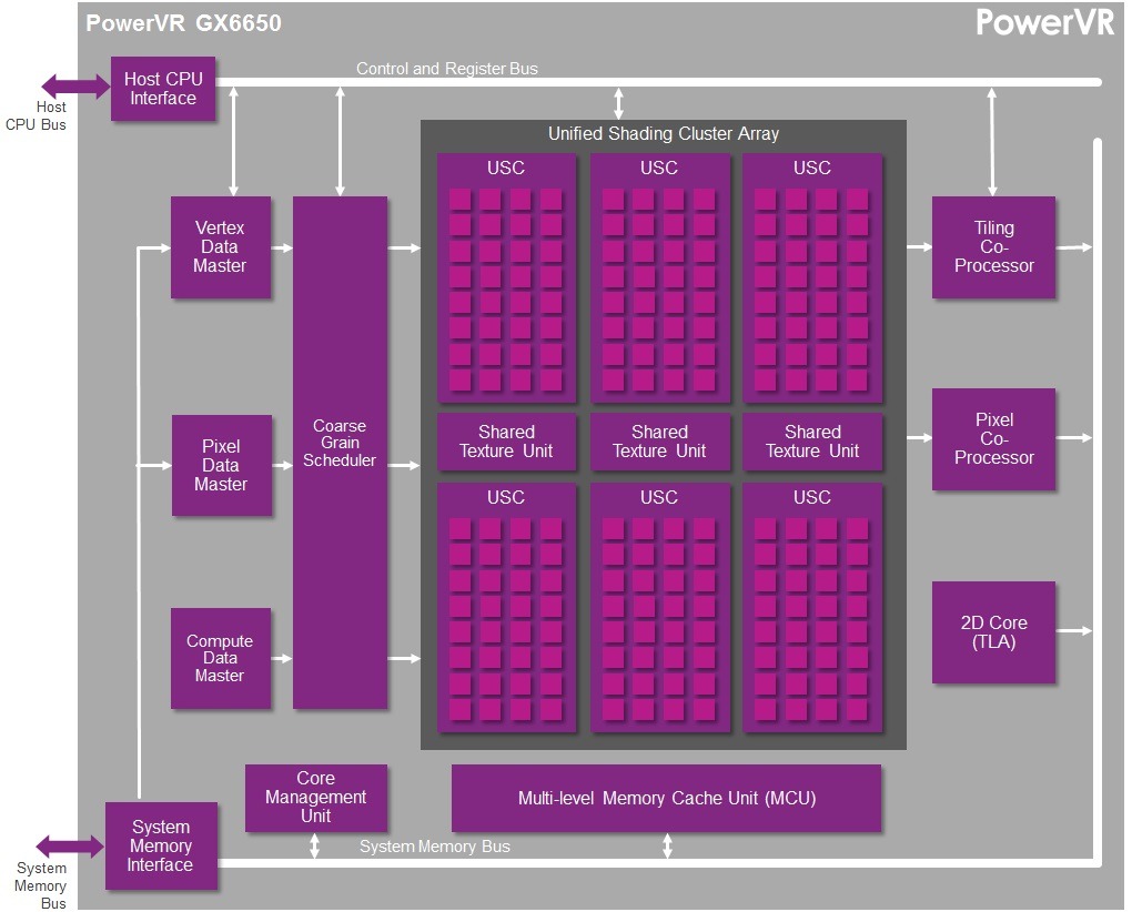
The Rogue architecture organises itself around a block — itself a number of other blocks — called the Unified Shading Cluster or USC for short. We scale the architecture to meet our customer’s demand for a GPU to fit their system-on-chip and the market segment it addresses, and we do that by connecting a number of USCs together, along with other associated resources, into the full GPU IP.
Lift the lid on a USC and you’ll see a collection of ALU pipelines that chew on the data and spit out results. We arrange those pipelines in parallel, 16 per USC. We do that because graphics is overwhelmingly a parallel endeavour where multiple related things, usually vertices or pixels, can be worked on at the same time. In fact, certain properties of modern pixel shading force parallel execution of related pixels together, so you always want to work on them at the same time.
Scalar SIMD execution and vector inefficiency
A key property of the USC’s execution is that it processes data in a scalar fashion. What that means is for a given work item, for example, a pixel, a USC doesn’t work on a vector of red, green, blue and alpha in the same cycle inside an individual pipeline. Instead, the USC works on the red component in one cycle, then the blue component in the next, and so on until all components are processed. In order to achieve the same peak throughput as a vector-based unit, a scalar SIMD unit processes multiple work items in parallel lanes. For example, a 4-wide vector unit that processes one pixel per clock would have a peak throughput equivalent to a 4-wide scalar SIMD unit that can process four pixels per clock.
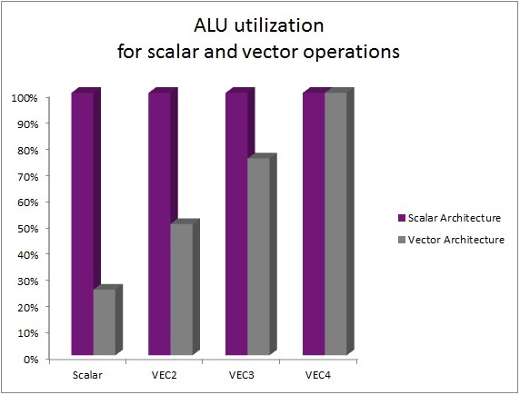
On the face of it this makes the two approaches appear to have equivalent throughput. However, modern GPU workloads are typically composed of data that uses many different data widths. For example, colour data typically has a width of 4 (ARGB), whereas texture coordinates might typically have a width of 2 (UV) and there are many examples of scalar (1 component) processing such as parts of typical lighting calculations.
Where data processing doesn’t fill the full width of a vector you waste the vector processor’s precious compute resources. In a scalar architecture, the types you’re working on can take any form and they get worked on a component at a time, in unison with their other buddies that make up the parallel task. For example, a shading program that consists entirely of scalar processing would execute at 25% efficiency on a 4-wide vector architecture but would execute at 100% efficiency on a scalar SIMD architecture.
Lots of power-efficient ALUs!
Let’s get back to the individual pipelines working together on the parallel task in the USC. We have 16 of them remember, but inside each pipeline, there’s actually a number of ALUs that can do work. We have 2 FP32 ALUs, 2 FP16 ALUs and 1 special function ALU.
Why dedicated FP16 ALUs? It’s for power efficiency in the main, but it also significantly affects performance. The reduced complexity of the logic in those ALUs lets us execute FP16 instruction groups at lower power than on the FP32 ALUs, all while giving a higher per-cycle throughput because of the extra operations they can perform. You’ll see what I mean there shortly.
Computation at lower precision is something that’s possible a lot of the time in modern graphics rendering, and there’s support for mixed precision computation in all of the popular graphics APIs Rogue is aimed at, and that includes Direct3D 11, as well as the much more common OpenGL ES2 and ES3 APIs. Not building a mixed-precision computational pipeline is a mistake in embedded graphics, because of the power efficiency gains it can realise via that commonality of mixed precision workloads.
Performance and capability
The ALUs aren’t equal in capability, so let’s cover what each can do so you can see what their performance is:
The FP32 ALUs in all PowerVR Series6, Series6XT and Series6XE cores are capable of up to 2 floating point operations per cycle. Per USC, that’s a peak of 64 FLOPs per cycle.
 There can be up to eight Unified Shading Clusters (USCs) inside a PowerVR Series6 GPU
The FP16 ALUs in PowerVR Series6 GPUs are capable of up to 3 floating point operations per cycle, and we’ve improved the FP16 ALUs in Series6XE and Series6XT to perform up to 4 FLOPs per cycle. Per USC, that’s up to 128 FLOPs per cycle depending on the product and which family it finds itself in. The improved design in Series6XE and Series6XT is additionally a bit more flexible, making it easier for the compiler to issue operations to that part of the pipeline.
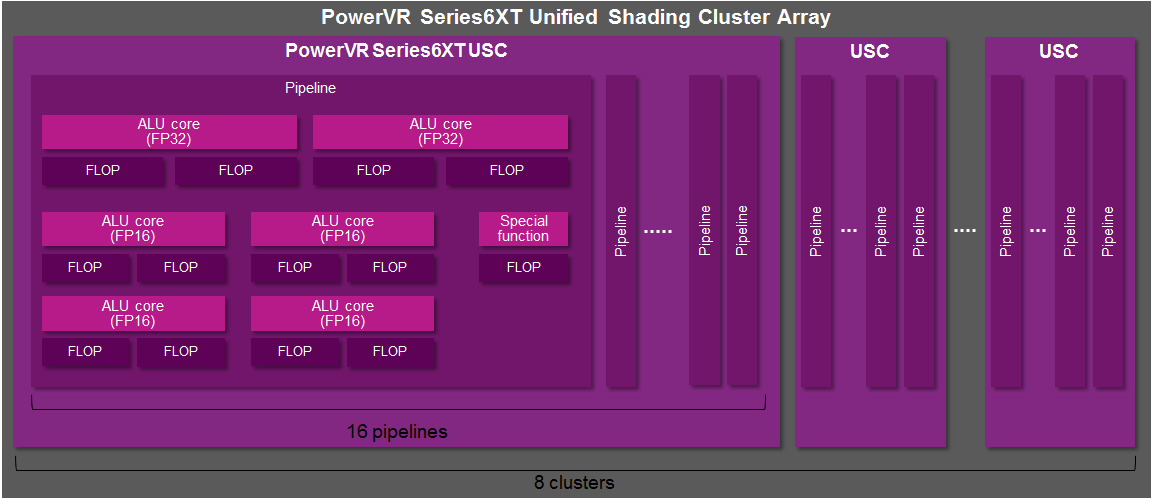 There can be up to eight Unified Shading Clusters (USCs) inside a PowerVR Series6XT GPU
Lastly, we have the special function ALU, which handles more complex arithmetic and trigonometric operations such as sine, cosine, log, reciprocals and friends, on scalar values. It has a range of output precisions and performance per operation that vary because of their nature.
Adding it all up into ALU cores
Now that I’ve described the Rogue compute architecture from the basic building block of the USC, down to how it executes using 16 parallel pipelines, each with significant dedicated compute resource, let’s count everything the same way our competitors do: as cores. That gives us 32 FP32 ALU cores, up to 64 FP16 ALU cores, and 16 special function ALU cores per USC.
The ALU core terminology is important when comparing Rogue to competitor products marketed in the same way, and we’d like everyone to stick to it as much as possible.
Finally, remember that we have 1-to-many USCs, depending on the product, in Series6, Series6XT and Series6XE. Here are two examples, to help verify how to total everything up:
PowerVR G6230: two Series6 USCs – 64 FP32 ALU cores with up to 128 FLOPs per cycle – 64 FP16 ALU cores with up to 192 FLOPs per cycle. That means up to 115.2 FP16 GFLOPS and up to 76.8 FP32 GFLOPS at 600MHz.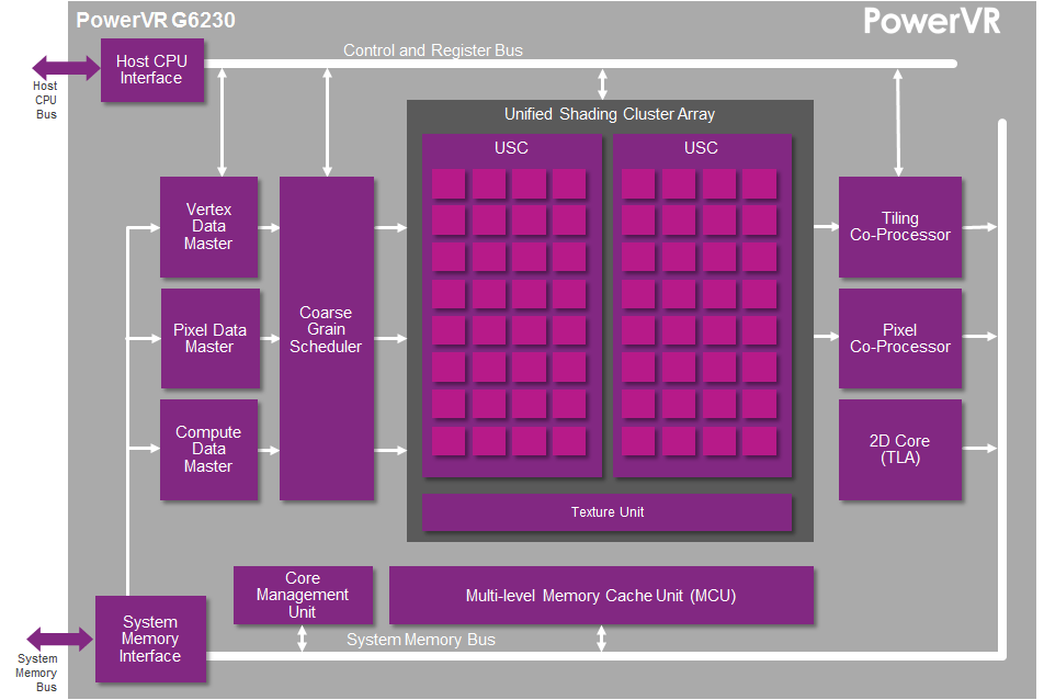
PowerVR GX6650: six Series6XT USCs – 192 FP32 ALU cores with up to 384 FLOPs per cycle – 384 FP16 ALU cores with up to 786 FLOPs per cycle. That means up to 460.8 FP16 GFLOPS and up to 230.4 FP32 GFLOPS at 600MHz.
Happy core counting!
If you have questions or want to know more about our PowerVR GPUs, please use the comment box below. Make sure to follow us on Twitter (@ImaginationTech) for the latest news and updates from Imagination.