- 06 November 2013
- Imagination Technologies
If you think of smartphones and tablets as the go-to devices for personal computing, you’ve probably wondered quite a few times how technology has evolved to the point where consumers can now run demanding applications that bring unique, feature-rich user experiences yet rely on mobile chipsets requiring a few watts of power.
The answer lies in efficient processing. All our hardware IP has been designed with a focus on efficiency, which means we are always thinking about how we can offer you the best performance for the lowest possible power consumption, making our technologies better suited for current and future workloads in mobile and embedded processing.
Building a processor architecture with efficiency in mind can have multiple implications. In this article we are going to look at how certain features of our PowerVR multimedia hardware IP are linked to the memory specifications of a typical mobile processor.
A crash course in memory hierarchy for mobile processors
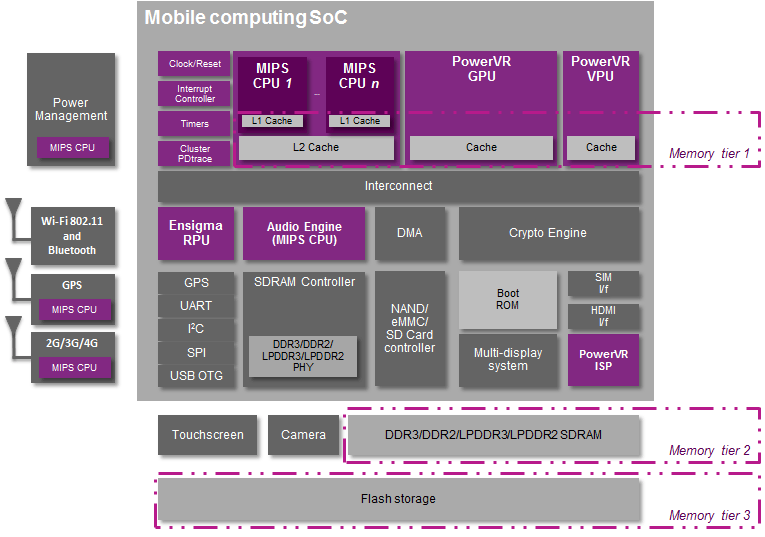
There are three layers of memory inside a mobile device. The first tier (cache or on-chip memory) is usually the most expensive but is the fastest in terms of time to access.
Modern CPU designs for mobile have at least three independent caches: an instruction cache (I-cache) to accelerate fetching executable code from RAM, a data cache (D-cache) to speed up data loads and stores, and a translation lookaside buffer (TLB) used for translating virtual to physical addresses. The data cache is usually deployed in a hierarchical structure (L1, L2, L3, etc.) inside a multicore CPU.
Mobile GPUs have a similar structure of cache memory. Inside a PowerVR GPU you will typically find L0, L1 and L2 caches around the unified shading engine (PowerVR SGX) or unified shading cluster (PowerVR ‘Rogue’), while the shared system level cache (SLC) will contain partitioned cache memory (Cache 0, 1, 2, etc.) for improved memory bandwidth.
The second tier is made of RAM (Random Access Memory); this is what manufacturers talk about when they announce new devices with N GB of memory. RAM usually refers to the fast memory used by applications to hold data and instructions. You can think of it as a relatively large filing cabinet for processing units in your mobile device to access information in a timely manner.
The third tier typically includes flash memory, which is several orders of magnitude slower compared to RAM and is primarily used as a large storage resource for MMCs (MultiMediaCard), SD memory cards, USB flash drives, solid-state drives, and similar products.
 A typical mobile processor architecture
In a smartphone or tablet, mobile DRAM memory is usually stacked on top of the chip while flash memory is a separate component on the board.
System architects can either use memory components from third-party suppliers (Synopsys, Cadence, etc.) who provide ready-made embedded memories or logic libraries or can build their own using memory macros from foundries such as TSMC or GLOBALFOUNDRIES. Some of the largest mobile RAM vendors include Elpida, Micron, Nanya, Rambus, Samsung, and many others.
Memory bandwidth is an important driver for power consumption
One of the highest users of power in SoCs (Systems-on-Chip) is off-chip memory traffic. According to Rambus, advanced multimedia applications (3D gaming, Full HD video decode/encode, augmented reality, etc.) push memory bandwidth requirements well above 12 Gbps. For a typical power consumption between 60-80 mW/Gbps for LPDDR3, total RAM power consumption due to increased memory traffic can go up to 1W or more, depending on the type of memory being used, its frequency, etc. To put that into perspective, a smartphone SoC will go up to around 1-2W of peak power consumption while tablets can go up to 4-5W; this means that power consumption due to memory traffic in a mobile processor can range from 25% to 50% of total system power.
This is because mobile SoCs usually need to process data in parallel and therefore must compete among their peers for access to RAM. If not planned correctly, both system- and unit-level design decisions can degrade system performance, increasing cost and power consumption. Brute-force, power-hungry processors will have an immediate impact not just on their individual efficiency inside the system, but are likely to affect a chipset’s overall performance because these designs will typically attempt to eat away at memory bandwidth at an accelerated pace.
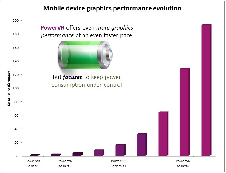
 The evolution of mobile graphics performance (2009 – 2014) for PowerVR Series4, Series5/5XT and Series6 GPUs
For example, when introduced at CES 2012, PowerVR Series6 GPUs offered an increase of more than 20x in performance compared to the single-core SGX-based devices that were shipping in large volume at the time. However, even more importantly, the 5x more efficient ‘Rogue’ architecture has integrated various features which help improve not just the overall performance of mobile and embedded devices, but enable several key power-saving mechanisms that keep thermal envelopes well-balanced.
By choosing the right IP blocks that have proven to reduce memory bandwidth and increase system efficiency, you can see tangible benefits in achieving smooth, solid performance while improving the lifetime of your device and lowering bill of materials (BOM) costs.
PowerVR Series6 ‘Rogue’: Improving memory bandwidth with TBDR and PVR3C triple compression
Our PowerVR IP technologies include graphics, video and ISP solutions which have been developed over more than 20 years to meet the most demanding requirements of high volume mobile and consumer applications. With their roots in consumer electronics and high-end PC graphics, PowerVR visual technologies lead the world in delivering exceptional levels of performance while maintaining the low power and high system latency tolerance principles of its initial architecture.
Our PowerVR vision IP is equipped with a series of market-leading, unique features that provide developers with a twofold advantage: ensure they are able to target platforms with reduced memory footprints and seamlessly enable their applications to consume less power when running on PowerVR-based devices.
If we look at the current crop of state of the art mobile GPU architectures, most of them go for a tile-based implementation to keep memory traffic to a minimum. On top of that, PowerVR has the unique advantage of deferred rendering.
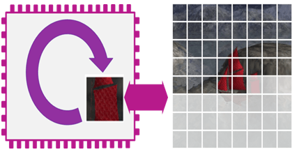
TBDR focuses on minimising the processing required to render an image
TBDR (Tile-Based Deferred Rendering) is an elegant solution to drawing only the visible elements in the scene, whereas all other implementations are Z-buffer based hybrids also known as Immediate Mode Renders; some of these IMR-based architectures go for advanced culling methods which are area- and power-expensive.
 Tile-based Deferred Rendering made easy with PowerVR
All parts of the TBDR are fully handled in hardware and are completely invisible to software developers, ensuring maximal compatibility and performance between our different GPU families. PowerVR’s unique smart parameter management technology allows TBDR rendering in limited memory footprints, ensuring compatibility of high complexity titles without excessive memory usage.
PVR3C triple compression offers lower power consumption and superior memory bandwidth efficiency
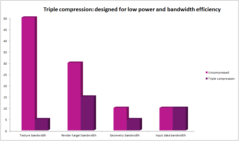
The first bandwidth-reduction feature in PowerVR Series5XT and Series6 cores is related to our support for the PVRTC2 texture compression format, at both 2bpp and 4bpp resolutions. PVRTC2 offers new features such as high contrast textures, NPOT support and sub-texturing and sits alongside our existing PVRTC format, which has been built into our hardware since the release of the PowerVR Series4 GPU family. PVRTC and PVRTC2 achieve between 8:1 to 16:1 compression for texture data inside games or augmented reality applications. Our PVRTC technology defines an efficient hardware texture decompression standard which minimizes bandwidth needed between the GPU and main memory, by enabling the graphics pipeline to maintain the texture in compressed form. Keeping the texture compressed at all times means the cache in the chip effectively becomes several times more effective. PowerVR GPUs only decompress texture data when needed in the final rendering process, resulting in significant reductions in on-chip and off-chip bandwidth and processing power. This is one of many reasons why support for texture compression has been, and continues to be, a key part of every generation of PowerVR graphics architecture, including all upcoming ‘Rogue’-based platforms.
Secondly, there are two types of distinct lossless compression integrated inside our PowerVR ‘Rogue’ architecture:
– Lossless geometry compression
This is included in all PowerVR ‘Rogue’ cores and compresses the intermediate geometry data as part of our updated tile-based processing. Geometry compression provides a 3:2 compression ratio, thus saving memory footprint, memory bandwidth, which in turn leads to lower power consumption.
– Lossless image compression (also referred to as Lossless Framebuffer (De)Compression FBC/FBDC).
 Triple compression technologies integrated in PowerVR ‘Rogue’-based GPUs
This optional component (included in PowerVR G6x30 cores) operates on uncompressed image/texture data flow. With lossless image compression, render targets can be written out by the GPU with compression (render to texture and framebuffer) and can be read back by the GPU with decompression (texturing). This means the GPU can save on both write and read bandwidth, typically seeing a compression ratio of 2:1 (but can be as high as 30:1 for blocks with constant colour). Textures are lossless compressed without extra effort by the developer as part of the texture upload by the GPU hardware. Decompression can be integrated as part of the display controller allowing final frame buffer writes and reads (by the display pipe) to be compressed leading to system level bandwidth saving.
This technology is particularly useful for browsers and certain GUI components cannot accept any quality degradation. In memory bandwidth constrained systems, lossless image compression obviously can also lead to higher sustained frame rates.
PowerVR video IP: architecturally designed for significant reductions in bandwidth
Video transcoding has been one of the main drivers for improving memory bandwidth in mobile SoCs. For example, video decoding in particular is a nondeterministic process; motion vectors may change significantly from one block to the next, so traditional bandwidth-saving techniques may not offer the promised theoretical reductions. These considerations and many more make designing a VPU (Video Processing Unit) a very complex process.
With the recent launch of our PowerVR D5500, the first 10-bit, multi-standard decoder compatible with the H.265 (HEVC) standard, we have introduced a new architecture designed to support the higher resolutions, frame rates, and bitrates of 4K resolutions while optimizing silicon area and bandwidth usage in line with today’s video codec requirements.
By being part of Imagination’s unique and comprehensive PowerVR family of visual IP cores, all PowerVR VPUs are designed to integrate fully with other members of the family such as the PowerVR SGX or ‘Rogue’ graphics IP portfolio under unified software. When combined with our mobile GPU IP, PowerVR decoders and encoders deliver a significant reduction in system bandwidth compared to alternative solutions through the use of sophisticated system integration features such as support for shared system level cache (SLC) with Imagination’s PowerVR graphics cores.
Furthermore, PowerVR VPUs have been designed to support high memory latency from the start. This is because our architects were aware that other processors in the system (CPUs, GPUs, etc.) needed to have their fair share of the memory controller in between the VPU fetching reference frames from main memory. By packaging up memory requests more efficiently compared to our competitors, PowerVR video cores reduce memory traffic and keep system power consumption in check.
In conclusion, even though performance in mobile has seen an incredible boost over the last decade, it is always important to think about other factors such as power consumption or memory bandwidth usage when designing processors. The reason is simple: with more and more functionality added to the mobile SoC, you have to make sure you are using every last bit of silicon as efficiently as possible and therefore guarantee the best possible user experience.
For more news on our PowerVR technologies, follow Imagination (@ImaginationTech) on Twitter and keep coming back to our blog.


